Global Wafer Level Packaging Market Analysis & Outlook 2030
-
Product Code:
RP-ID-10352025 -
Published Date:
21 Oct 2022 -
Region:
Global
-
Category:
Packaging -
Publisher:
Pub-ID-54
Impact Analysis on the Growth of Market
Inflation and Looming Recession to Haunt Businesses:
In 2022 & 2023, market players expected to sail in rough waters; might incur losses due to huge gap in currency translation followed by contracting revenues, shrinking profit margins & cost pressure on logistics and supply chain. Further, U.S. economy is expected to grow merely by 3% in 2022.
....
The Research Report is Updated with 2022 Base Year, 2023 Estimated year and Forecast till 2035 with Market Insights.
With the dip in global production, the GDP has contracted in 2020 and impacted the market across the world. Upon placing a Sample Request, you will receive an updated report with 2022 as base year, 2023 as estimated year and forecast to 2035. This will have market drivers, recovery rate in the market, insights and competitive analysis.
Market Overview:
Translate Report
The wafer level packaging market is anticipated to expand at an annual growth rate of 20% over the period 2022-2030, and the global market is expected to reach USD 6 billion by 2021.Wafer level packaging (WLP) is used in the production of electronic components such as resistors, capacitors and transistors. Build integrated circuits on a single chip that houses a soldering iron on a wafer. WLP devices simplify the manufacturing process by integrating wafer fabrication, filling, testing, and baking to the wafer surface. WLP offers several advantages such as multi-chip capability, higher input/output densities, smaller form factors, improved electrical and mechanical performance, higher cost/performance efficiencies, and the possibility of advanced 3D structures.
Wafer Encapsulation Growing demand for fast and compact electronic devices compared to traditional encapsulation technologies such as tray encapsulation and wire encapsulation is driving the demand in the wafer packaging market. Also, the Internet of Things (IoT) is very popular and is the third wave of technology. The rapid development of the chip level packaging industry is expected to be driven by the growing popularity of the Internet of Things and mobile electronics markets. Additionally, the technological advantages of WLP over traditional packaging technologies and the urgent need to reduce circuitry in microelectronic devices are driving the growth of the chip-level packaging market. However, packaging a large WLP sector is difficult and high initial investment is a major constraint on the market. The growing demand for faster, lighter, smaller and cheaper high-performance electronic packaging solutions is an opportunity for the electronics market.
The demand for chip-level packaging is driven by Jiangsu Changjiang Electronic Technology Co., Ltd. and Fujitsu Limited, which are expected to come from large R&D investments by several large corporations. This will improve the quality of the package. For example, in April 2016, Deca Technologies announced the signing of an agreement, but ASE plans to invest $60 million in licensing WLP technologies and processes for the DecaM series.
Global Wafer Level Packaging Market Scenario:
A key feature of wafer level packaging is it’s interconnect technology useful for multiple applications. The diverse applications of the Internet of Things in industries such as ICT, electronics, automotive, industrial and medical have generated interest in chip-level packaging. WLP fans are expected to be the fastest growing in the wafer surface packaging industry because of their high density and the ability to integrate multiple heterogeneous shapes in a single, affordable housing with good electrical performance. However, this technology is limited to a limited number of applications and the chip package requires some cellular bandwidth. However, mobile phone customers have high demand for miniaturization and integration, while at the same time lowering the cost of the packaging market to a more attractive level.
Technological advantages of state-of-the-art packaging over conventional technologies: Technological advances in electronic packaging have enabled highly efficient and reliable electrical connection solutions for electronic products, increasing the demand for slice-level packaging. Wafer-scale packaging offers many advantages over traditional wired packaging, including superior thermal and electrical performance, substrate flexibility for different performance requirements, and robust experience with manufacturing and processing equipment. WLP is also an economical and innovative process that appeals to electronics customers and packaging designers to maximize package performance.
Geography Analysis:

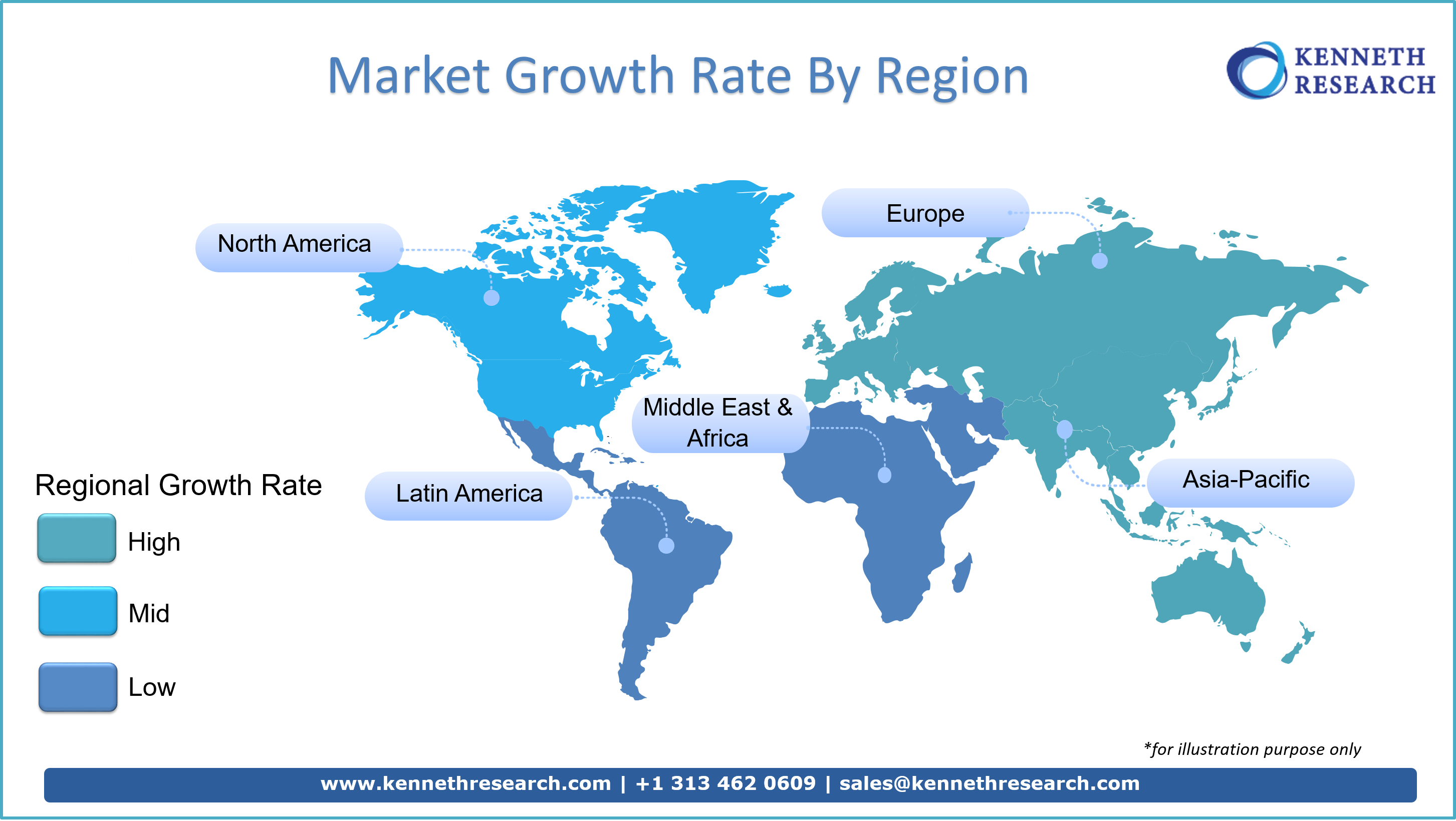
The report further discusses the market opportunity, compound annual growth rate (CAGR) growth rate, competition, new technology innovations, market players analysis, government guidelines, export and import (EXIM) analysis, historical revenues, future forecasts etc. in the following regions and/or countries:
- North America (U.S. & Canada) Market Size, Y-O-Y Growth, Market Players Analysis & Opportunity Outlook
- Latin America (Brazil, Mexico, Argentina, Rest of Latin America) Market Size, Y-O-Y Growth & Market Players Analysis & Opportunity Outlook
- Europe (U.K., Germany, France, Italy, Spain, Hungary, Belgium, Netherlands & Luxembourg, NORDIC(Finland, Sweden, Norway, Denmark), Ireland, Switzerland, Austria, Poland, Turkey, Russia, Rest of Europe), Poland, Turkey, Russia, Rest of Europe) Market Size, Y-O-Y Growth Market Players Analys & Opportunity Outlook
- Asia-Pacific (China, India, Japan, South Korea, Singapore, Indonesia, Malaysia, Australia, New Zealand, Rest of Asia-Pacific) Market Size, Y-O-Y Growth & Market Players Analysis & Opportunity Outlook
- Middle East and Africa (Israel, GCC (Saudi Arabia, UAE, Bahrain, Kuwait, Qatar, Oman), North Africa, South Africa, Rest of Middle East and Africa) Market Size, Y-O-Y Growth Market Players Analysis & Opportunity Outlook
.


